News Story
Phosphorene: 2-D material ripples, giving optical properties
Complete examination of optical and spin properties of 'graphene's cousin'
UMD physicist Ian Appelbaum and postdoc Pengke Li throughly examined a new 2-d material called phosphorene. Like its famous cousin graphene, this material is called 2-d because its structure is only one atom thick though it can be made both long and wide.
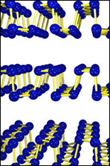
Unlike graphene, phosphorene is not entirely flat. Its honeycombed molecules fit together in a rippling shape, which means that light entering the molecule can take different directions. This effect might be used in optical computing or in microsocopy.
Phosphorene's rippled arrangement means that the spin of the electrons is stabilized, which could make the material more useful than graphene in spintronic applications.
The authors recently published their work in the journal Physical Review B.
Author Summary
We present a symmetry analysis of electronic bandstructure including spin-orbit interaction close to the insulating gap edge in monolayer black phosphorus (“phosphorene"). Expressions for energy dispersion relation and spin-dependent eigenstates for electrons and holes are found using the mathematics of symmetry operations, or “group theory”. Importantly, we expose the underlying symmetries giving rise to substantial anisotropy in optical absorption, charge and spin transport properties, and reveal the mechanism responsible for valence band distortion and possible lack of a true direct gap.
Structural features
Phosphorene has a honeycomb lattice of identical atoms just like graphene. However, due in part to the fact that phosphorus has 5 valence electrons (not 4 like carbon), it is not perfectly planar but rather rippled along buckled rows in a particular direction. One consequence of this geometry is that for the important valence band state, different atomic orbital coupling gives vastly different dynamical response (“effective mass”) to forces of the same magnitude but oriented orthogonally in the plane.
Electro-optical properties
Unlike the semimetal graphene, phosphorene is a semiconductor that shows large changes in conductivity upon optical absorption of photons with enough energy to exceed the insulating bandgap. The full structural symmetries we analyze, including especially the in-plane anisotropy provided by the buckled rows, enables efficient electronic optical polarimetry, where the phosphorene layer will absorb only photons of a certain linear polarization, and allow an electronic measurement.
Electron magnetic moment: “spin”
Further comparison to graphene is again useful when considering spin-electronic, or “spintronic”, applications. Although spin-orbit interaction (which mixes the spin information) is weak in graphene, spin lifetime is very short because (like most other 2D materials) out-of-plane atomic vibrations couple strongly to the spin-flip process. Phosphorene’s anisotropy (absent in graphene) gives rise to a previously unexpected result: for spins oriented in the plane, lattice symmetry forbids spin flips due to this mechanism! We therefore predict that spin lifetimes are much longer in phosphorene than in graphene.
Further research:
One consequence of the atomic buckling is that for multiple layers, there are several stacking arrangements possible. One potential future research direction is to explore the symmetry-induced consequences of each.
Other 2D materials are also of potential interest. There are many other "-ene"s: Si, Ge, and Sn have already received much attention by the research community, but none can be exfoliated from a bulk crystal like graphene (from graphite) and phosphorene (from black phosphorus). Other group-V materials are possible, but one has to be careful experimentally... Apparently Nitrogen forms a black-phosphorus phase, but this allotrope is explosive!
Published October 3, 2014
Recent Stories
Stories / Jul 10, 2026
MATRIX Helping Maryland Build Tomorrow's Workforce

Stories / Jul 8, 2026
Solid Oxide Fuel Cell Breakthrough

Stories / Jul 1, 2026
Establish Research Partnerships at the MATRIX Open House

Stories / Jun 26, 2026
Interdisciplinary team receives UMD Grand Challenges Impact...

Stories / Jun 25, 2026
Aircraft May Refuel Themselves - With Help From AI

Stories / Jun 25, 2026
MEII Director serves on Daily Record virtual panel discussion

Stories / Jun 24, 2026
Dean Graham Reappointed to Second Five-Year Term

Stories / Jun 8, 2026
Alchemity receives Build our Future Award from Governor Moore

Stories / May 28, 2026
Generations of Graduates: A Full-Circle Celebration

Stories / Apr 27, 2026
New Lecture Series Unites Experts to Solve Critical Challenges
